A Lot of Effort to be Thrown Away: Sega's Dottori-kun!
You might have heard the term “discrete logic” before. What does that mean, and how can you use discrete logic to make an image? And if that wasn’t enough, imagine making a video game; a physical object, a small self-contained computer, just to throw it away. These are the themes of today’s blog post!
Sega’s Dottori-kun
Let’s start with the more fun topic; Sega’s Dottori-kun. Imagine, if you will, a game where you control a hero in a maze, collecting dots, and avoiding an enemy bent on hunting you down and crashing into your player. Sound like Namco’s 1980 Pac-Man? Of course not! We’re talking about Sega’s 1979 Head-On.
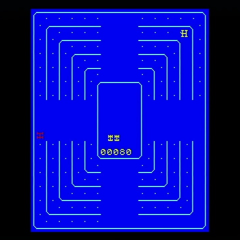
This screenshot is from the Sega Saturn’s Sega Ages Memorial Collection Vol. 1, but it’s a very faithful port. So, if in 1979 Sega was releasing dot-collecting video games that look like that, why was Sega releasing a game– an arcade title, in fact– that looked like this in 1990?
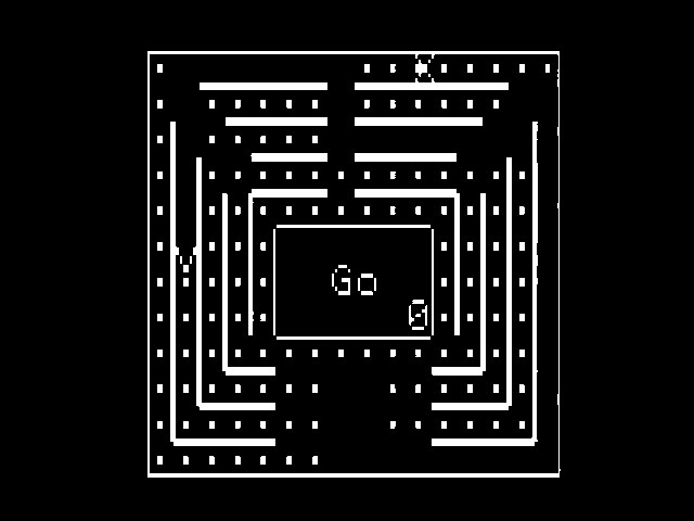
This is Sega’s Dottori-kun. (Note that these photos are heavily touched up, as I had a hell of a time capturing this video) If the monochrome graphics in 1990 didn’t tip you off that this isn’t just a normal arcade board, perhaps the fact that the game doesn’t accept coins, and its attract mode looks like this, will:

Sega’s Dottori-kun exists, according to internet lore, because of Japan’s Electrical Appliance and Material Control Law. This law still exists today, and what you find online about it seems to imply that a major portion of it has to do with assessing electrical devices for meeting various requirements.
In the 1990s, a big part of Sega’s arcade business was selling cabinets like the Astro City that didn’t come with game boards included. Dottori-kun seems to exist primarily to provide a simple game that could be used for assessment in line with Japanese law. It was included with the cabinet as sold (likely because the cabinet had to be in the same state as assessed for it to be valid), but was not usable for an arcade operator beyond basic testing that the game board worked, it would just be thrown away or maybe saved to be scavenged for parts.
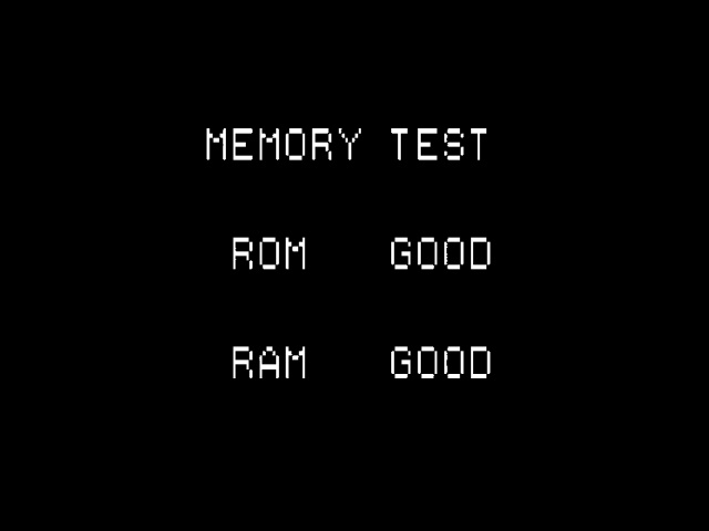
And that’s really it. Dottori-kun even includes a simple test mode, which could allow an operator to verify that their cabinet worked before plugging an expensive recent release like Fighting Vipers into it. It does reveal a little secret:
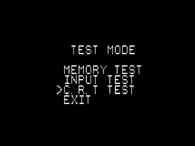

Yes, the Dottori-kun game board, despite its game being monochrome, can actually display some simple colors. This actually makes sense; a JAMMA video signal is made up of separate Red, Green, and Blue components; there’s no option for monochrome, and no need to generate a complex color burst like you might for composite video. But it’s interesting that Sega didn’t use it to make Dottori-kun look a little more like its 1979 inspiration.
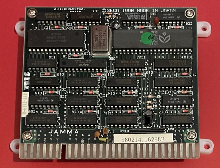
And here is our segue: the Dottori-kun board. Other than a CPU, a ROM, and a small amount of RAM, this board is entirely made up of discrete logic. But… just what are the Orcos?!!!!!
Discrete logic
You probably have some idea that there’s something called a “transistor”. A transistor is basically a voltage-controlled switch; current can only flow from one point to another (generally, the collector and emitter) if there’s a voltage on another point, called the base.
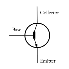
This is an NPN transistor; there are many variants. And that’s because transistors, the base unit of digital electronics, are actually analog devices. They can have many different use cases; for example, the Apple II relay project used a transistor to allow the 5V signal from the Apple ][’s disk drive to control a more powerful 12V signal; this is an entirely analog process, since you can see that it depends on more than one different voltage.
Transistors are also used to create the base units of digital computing. If the processor you’re using to read this post isn’t based around transistors, let me know. (And if it’s based around relays, send me an audio recording, I’m sure those clicks are glorious) But transistors are kind of an inconvenient base unit for many purposes; sure, you can build anything out of a bunch of transistors, but you don’t really want to.
Boolean logic
When mathematicians sit down to design a theoretical processor, they might use something called boolean logic. Boolean logic, named for the mathematician Boole, maps well onto digital computing, because it deals with things that are either on or off; oftentimes called “true” or “false”. But we could just as easily call them “0V” and “5V”. Boole taught us the valuable lesson that you don’t need to count very high to be a mathematician.
A typical example of a Boolean logic is the “AND” gate. It’s called a gate, but you could imagine it as a function too if that’s easier. A typical AND has two inputs, and one output. Everything is Boolean, it can only have two values. If the inputs are both “true”, then the output will be “true”. If any of the outputs are “false”, the output will be “false”. An AND gate is symbolized with a “&”, or sometimes a “^”. Since I use ^ to denote exponents, we’ll stick with the ampersand.
An “OR” gate, the partner of the “AND” gate, will return “true” if any of its inputs are “true”; it only returns “false” if both of its inputs are “false”. Its sibling the “XOR” (or “Exclusive OR”), will return “true” if only one of its inputs are true, and “false” if none of them are “true”, or if they both are.
Boolean logic gates don’t need to have two inputs. An “inverter” is a gate with one input and one output. If the input is true, the output is false. If the input is false, the output is true. A “buffer” just outputs what you input. If you put an inverter on the output of an AND gate, it becomes a “NAND”, or not-AND, gate. The same logic can give you “NOR” and “NXOR” gates.
You can even create an AND gate with more inputs; a three-input AND gate, for example, will only return “true” if all three inputs it has are “true”, a four-input OR gate will only return “false” if all four of its inputs are “false”, and so on.
Discrete logic gives you chips that give you these kinds of basic building blocks. They’re massively produced and used pretty much everywhere as “glue logic”; for major processors it’s worth having chips manufacturered, but if you just need some simple gates it’s a lot cheaper to buy a logic chip that already exists.
Example use of discrete logic
Here’s a simple example. Let’s say we have a 6502 processor, which has 8 data lines, and 16 address lines. The 6502 can access 64kiB of RAM (2^16 = 65,536), therefore. But let’s say we have a 16KB RAM chip we want to attach. Since it has only 16KB of addressable memory, it only has 14 address lines. (2^14 = 16,384) What do we do with those extra two address lines, A14 and A15?
At first, you might think that we might just not attach them. But this causes a problem.
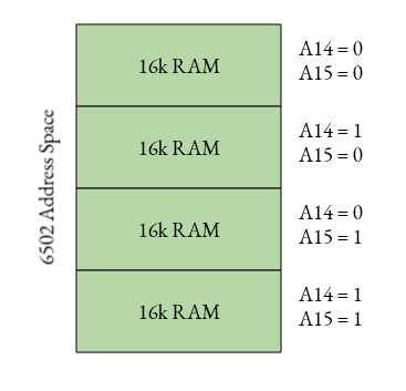
Notice that no matter what, we always are connected to the 16k of RAM; we now can’t connect anything else to our 6502, so no ROM or peripherals. Even worse, we still only have 16k of RAM, so that extra space is basically being wasted. This is called a “mirror”, since any changes in the first 16k will be reflected in the other three.
Thankfully, memory chips usually have a signal called OE'. This stands for “Output Enable”, and the dash next to it means that it’s “active-low”; the output is enabled when the signal is zero. What if we hooked up the output enable to A15? Then we’d get this:
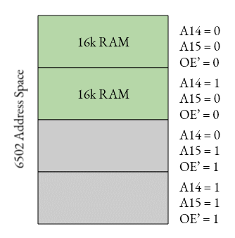
We now have 32kiB free for something else; on a 6502, this would usually be ROM. This might be good enough, if you don’t need that extra 16k, you could save some money and just print your design here, keeping one mirror around. But if you need all the 64k, then you can connect OE' to an AND gate.
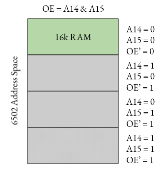
This is just an example; you could consider how this might work if you wanted the 16k somewhere else in the address space, other sizes of memory, or more complicated setups. But essentially, this is what “glue logic” is; a few simple pieces of logic that “glue” together more complicated chips like CPUs or RAM.
The Dottori-kun board

Let’s take a look at the photo of the Dottori-kun JAMMA board from before. With the connector at the bottom, we can see six rows of chips, so let’s see what those all are.
Top Row:
- SN74LS10N: 3 three-input NAND gates
- HD74LS02P: 4 two-input NOR gates
- 74HC32N: 4 two-input OR gates
- SN74LS14N: Six Schmitt-Trigger inverters
Second Row:
- MPR-14479A: Sega Mask ROM
- 4.0000MHz oscilator
- Zilog Z80 CPU
Third row:
- SN74LS74AN: Two D-type flip-flops
- LC3517BS-15: 2048 bytes 8-bit static RAM
- SN74LS166AN: 8-bit shift register
- SN74LS245N: Octal bus transceivers
Fourth row:
- HD74LS00P: 4 two-input NAND gates
- SN74LS161AN: 4-bit binary counter
- SN74LS157N: 2:1 multiplexer
- SN74LS244N: Octal buffers, hooked up to the controls
Fifth row:
- SN74LS08N: 4 two-input AND gates
- SN74LS161AN: 4-bit binary counter
- SN74LS157N: 2:1 multiplexer
- SN74LS174N: Six flip-flops; this controls the 3-bit RGB colors for foreground and background
Sixth row:
- SN74LS161AN: 4-bit binary counter
- SN74LS161AN: 4-bit binary counter
- SN74LS157N: 2:1 multiplexer
- SN74LS157N: 2:1 multiplexer, used to control four video outputs (RGB and Sync)
It looks like this is a 4.00MHz Z80 computer with 2KB of RAM; by comparison, the 1977 TRS-80 Model 1 had a 1.77MHz Z80 and started at 4KB of RAM. So these specs aren’t at all impressive for 1990; but of course, this was a computer designed to be thrown away. Still, that CPU and its clock speed are the same as that in the Sega Master System, which was still a going concern at the time, and it has as much RAM as the work RAM on the base Nintendo Entertainment System.
I wanted to make a schematic and draw out how the computer here works, but it turns out there’s no reason to; Chris Covell has done a great job, and has a full disassembly of the game and schematic for the board on his site. So I’ll just go over some of the highlights; check out his site for the full details, and even a ROM hack to add some more features to the game and make it more Pac-Man than Head-On.
First off, we can see a few more types of logic chips here beyond the AND and OR gates I talked about above. Let’s go into some detail.
Binary counters
The binary counters are really the heart of the machine. So what is a binary counter? Essentially, a binary counter has a clock input, and counts up on each cycle of the clock. A 4-bit counter like the SN74LS161AN can only count as high as 16 (2^4), however, you can combine them by putting one’s output into the next input. This means that with four counters, we can go as high as (2^(4*4)) = (2^16) = 65536.
The counters are hooked up to the 4.00MHz clock, and are constantly counting up. This means that it will reach 65536 every (1/61) seconds; that last signal is therefore 61Hz. This is pretty close to 60Hz, and so it’s our vertical line frequency. One of the flip-flops (one bit of memory) is used to control an interrupt to tell the CPU to start working on a new frame, and the count restarts.
The CPU slows down
Interestingly, the 4.00MHz is not the clock speed of the CPU. The 4.00MHz is combined with an OR gate, slowing down the clock. When the clock is stopped, the discrete logic grabs the RAM and loads up the shift register. The shift register controls whether the foreground or background color is displayed for the next few bits, while the CPU is given a bit more time.
This means that unlike, for example, the Sinclair ZX80, the CPU does not control the video output; this is more like the Apple ][ line, though much simpler (and without artifact color, of course). The top 1.5KB of RAM are used for the screen, so this has no sprites, and a resolution of 128x96. (It’s actually linedoubled; each alternate line fetches the same data before moving on) The Apple ][ was able to take advantage of its slow 1MHz clock and a quirk of the 6502 that it only accesses RAM on half of each clock cycle, while the Z80 expects full access to RAM, so it has to have its clock halted to share.
This is why many game consoles like the NES and Sega Master System used a separate video RAM; in the Master System, the Z80 does actually get to run at a full 4.00MHz, because the Video Display Processor (VDP) has its own RAM that the CPU can’t access directly, and must go through the VDP to modify.
Why is the signal so hard to lock onto?
So a fun thing here is that I had a lot of trouble getting this video to capture. I thought I could use my GBS Control; after all, it’s designed for arcade signals. But it simply refused to lock onto the sync. You can see the maze, but it’s definitely not stable. Let’s see if we can find out why.

61Hz is a bit out of spec, but not that much worse than other systems play with. Additionally, the HSync frequency uses that 4MHz divided by 256; that makes it 15.62kHz, while in NTSC-land 15.734kHz is the frequency. Still, that isn’t far off from the 15.625 kHz signal that PAL territories used.
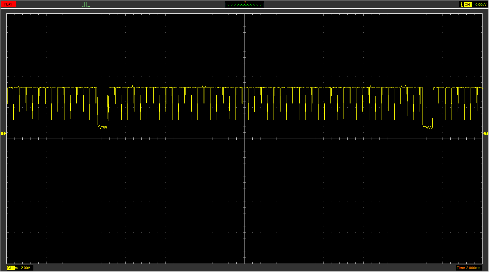
Let’s take a look at the sync signal. For this, I’ll be using my oscilloscope. My oscilloscope isn’t great; you’ll see from the signal that some pulses are being lost, but it will tell us enough.
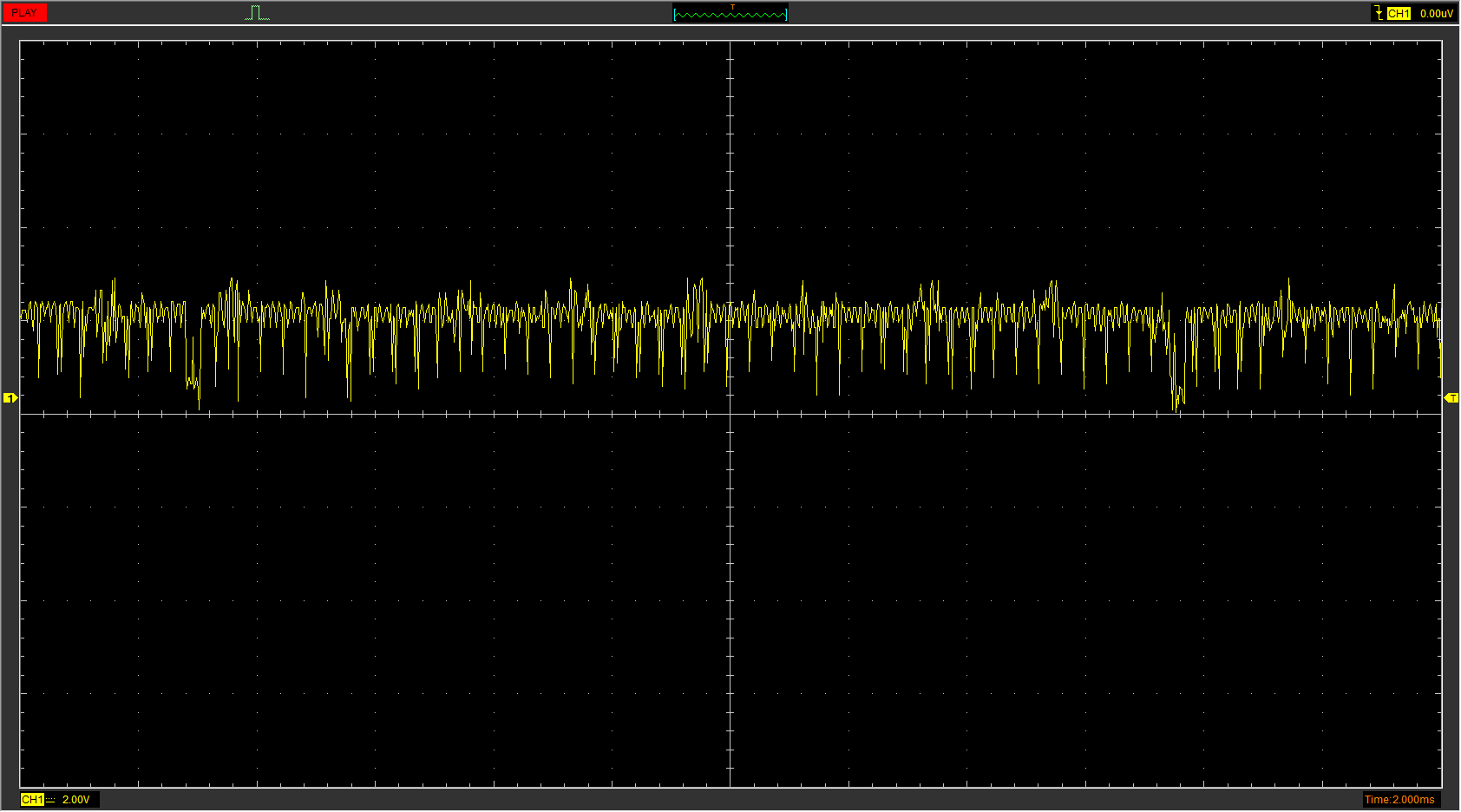
This is what’s called a “Composite” sync, or “CSYNC” to distinguish it from composite video. Each thin pulse is the 15kHz signal signifying a new line. Where the whole signal goes low, it’s the vertical blanking period, and you see no pulses. But that’s not quite right. Let’s compare to a working board, the pirate King of Fighters ‘97.
For one thing, this signal is much noisier; and yet, it is a better signal than the above, because I have no issues locking onto it. They were taken using the same procedure, so I think that noise is real; it is a pirate board after all. (Remember my oscilloscope is also not capturing at a high enough frequency to get all the detail)
Despite the noise, we can see that the horizontal sync pulses do not stop existing in the vertical blanking period. It looks like these missing pulses are making it so the GBS-8220 can’t lock on properly. I’m not sure if it’s something the Control firmware can fix or not; I don’t think anyone will be in a rush to make Dottori-kun work.
But why
I showed you a bad signal, but I didn’t tell you why. Let’s take a look at SN74LS157N, which I said controls the four signals. This is a “2:1 Multiplexer”, so it’s a bit complicated. Let’s take a look at the pinout. Note that putting a bar over the input symbol is the same thing as the ' I mentioned earlier; the dash is just easier to do in text.
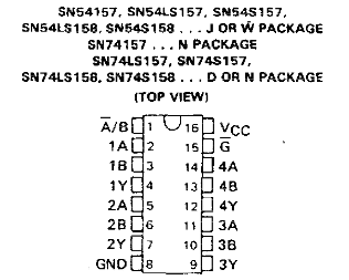
This consists of 4 multiplexed outputs. For example, 1Y will output either 1A or 1B, depending on the A'/B pin’s status. (If it’s high, it will output 1B. If it’s low, 1A) For the red (2Y), green (3Y), and blue (4Y) signals, the color selected for the foreground and background determines what the A and B signals are, and the A'/B signal has the pixel for each point put through from the shift register, which lets us know whether to output the foreground or background.
However, for the sync, 1A and 1B are connected together, and they’re both connected to the horizontal sync pulses. This means that 1Y, the sync output on the JAMMA connector, will always output the horizontal sync. So how does the vertical sync get involved at all?
You might notice that G' input. This is called the “strobe”; it’s a bit confusing, but for the 74LS157, if the strobe signal is high, all of the outputs will go low, regardless of what the other pins are. Therefore, the vertical sync controls G'; when it’s time to send a vertical sync pulse, the G' goes high and the sync, along with everything else, goes to zero.
This gives you a signal that doesn’t meet the specs of JAMMA. But it didn’t have to; Dottori-kun came with an arcade cabinet; as long as the particular monitors Sega used could lock onto the signal well enough to show a picture, then whether it supported some upscaler that wouldn’t exist until decades in the future didn’t matter, nobody was really supposed to play the game.
Dottori-kun!
I hope you enjoyed this look at a weird bit of Sega history, and got a chance to dig into some discrete logic. Dottori-kun is as simple as it gets; later on, I’m hoping to cover some boards that implement far more complex graphics circuits, including not only a proper sync, but more colors and hardware sprites using primarily discrete logic! And of course, this is just how integrated circuits work too; the logic is all on a die, but there are still things like or gates, shift registers, and counters inside.
Until next time, may your ROM and RAM be good!
