What made the NES so interesting?
I often like to cover oddities here; details of computers and arcade systems people may not have heard of, that didn’t sell well but had unique or interesting characteristics. But focusing on oddities like that can disguise the fact that sometimes, even systems that were very popular can stand out for unique design. Such be it with the Nintendo Entertainment System: had Nintendo’s console flopped, it’d definitely have a post already. But it doesn’t. Let’s fix that! And answer a simple question I was asked: what’s the deal with special chip games?
The Famicom
The Family Computer was Nintendo’s first console with interchangeable games. Releasing in 1983, just a year after 1982’s Donkey Kong Jr., the first Nintendo arcade game to be developed entirely in-house, without help from Ikegami Tsushinki. (Though they may have peeked at the prior boards just a bit, and got sued just a bit, but that’s another story) And isn’t it adorable?
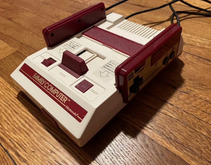
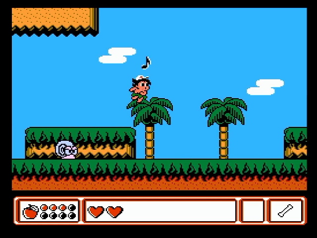
The interesting thing about the Famicom is that it was released in 1983, and its last licensed game in Japan, Master Takahashi’s Adventure Island IV, came out in 1994. The last licensed game, Wario’s Woods, came out in 1995 in Europe. That’s a long lifespan, and unlike the PC Engine, whose last licensed game Dead of the Brain Vol. 1 and 2 came out after a several-year drought, the Famicom was continuously getting more and more games. (Between unlicensed titles, the NES-on-a-chip and homebrew, it has never really stopped, either)
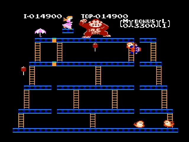
Think about the Famicom launch title Donkey Kong. It’s a reasonable arcade conversion, with high quality graphics. But much like the ColecoVision pack-in, it only includes three of the arcade game’s four levels, and none of the interstitials (“HOW HIGH CAN YOU GET”). It has 16kiB of program ROM and 8kiB of character ROM (just like Aspect Star “N”).
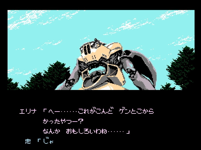
The largest game, HAL Laboratory’s 1991 Metal Slader Glory, dwarfs even Adventure Island IV with 512kiB of program ROM and 512kiB of character ROM. Its MMC5 mapper chip allows for a ton of advanced features. As for the game itself, it’s a text adventure with some stunning graphics, especially when viewed on a CRT.
But most people know this. The Famicom and NES benefitted from chips– like the aforementioned MMC5– inside the cartridges that expanded the system’s capabilities. For example, even a more modest title like Championship Bowling uses a “CNROM” board, which allows for larger graphics ROMs than the 8kiB limit; in this case, 32kiB, four times the graphics space.
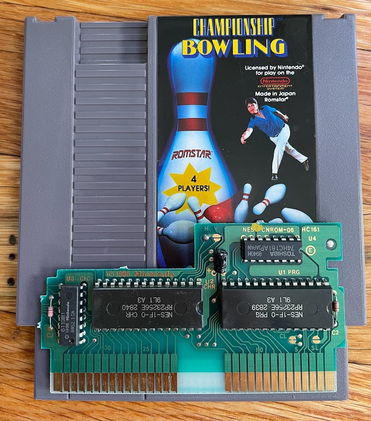
Have you ever wondered, though, what that means, exactly? What are these additional chips doing? And why did we see this on Nintendo’s consoles more than any other manufacturer?
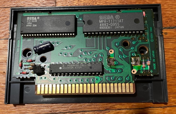
Here’s the inside of the most sophisticated Sega Master System game, Phantasy Star. It’s got a larger program ROM (with a mapper to help out), and a smaller, battery-backed RAM chip. But it offers no technical enhancements to the Master System hardware; graphically, Phantasy Star is unable to do anything that launch-title Teddy Boy couldn’t have done; it can just do more of it with that big beefy ROM. Championship Bowling is digging into the deep internals of the graphics side of the system in a way Phantasy Star simply can’t. (Or, depending on your point of view, doesn’t need to)
Cartridge ports
The Fairchild Channel F used the Fairchild F8 CPU, which had kind of a strange architecture with no address bus per se. So let’s switch to the Atari 2600.
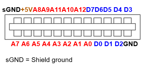
The Atari 2600’s cartridge port is a model of sheer simplicity. 13 address lines allow for 8kiB of gaming action– well, actually, A12 needs to be used as a chip select, so 4kiB of gaming action. There’s an 8-bit data bus, 5V for power, and grounds. That’s all you need, right?
Wrong. The Atari 2600’s cartridge port is actually very limited, and couldn’t even do Phantasy Star above. It’s missing a pin on the 6507 CPU called “R/W”; this means that the Atari cartridge has no idea when the game is reading or writing from memory. This is fine for a ROM chip, which can’t be written to anyway. But what if you wanted to put RAM on the cartridge? After all, the 2600 only has 128 bytes built in. You can’t do it. Not in a straightforward fashion, anyway.
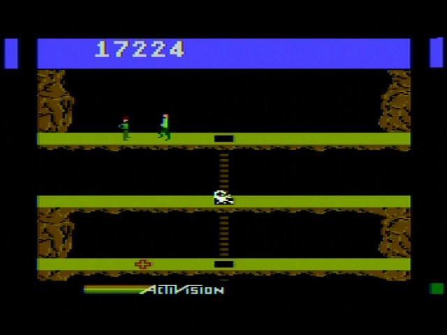
Well, of course, people found ways around these limitations. Without them, we wouldn’t have Pitfall II (Atari home computer version, not the 2600, pictured above) But it made things pretty complex to juggle when you had such a small window for your ROM to begin with.
Not only does the Master System have a larger address space for cartridges (thanks to its Zilog Z80, rather than the MOS 6507), it sent nearly all the signals from the Z80 out to the cartridge, including read and write signals. This allows for Phantasy Star’s save RAM– plus, all of this was also true of the predecessor to the Master System, the SG-1000, which had RAM expansion on at least one title, The Castle.
The NES went even further than that.
CHR
What do the ColecoVision, the Sega SG-1000, and the Master System all have in common? They all have the same amount of VRAM (Video RAM), 16kiB. This is because they have (more or less) the same video chip; and the TMS99xx video chip was very sophisticated for its time, allowing for cheaper dynamic RAM. In fact, back in 1979, that 16kiB formed the bulk of the RAM for TI’s TI-99/4A computer.
What is video RAM? It’s a solution to a serious problem. A video signal on the NES is a composite signal, ~60Hz in NTSC regions, ~15kHz line rate. Something like this.
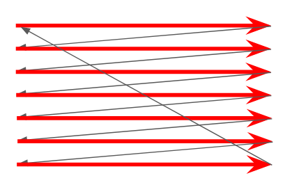
The key thing to note about this signal, though, is that the video processor must constantly output its signal. It can’t be early, it can’t be late, it can’t take a break. This means if there’s a conflict between the processor wanting to use RAM, and the video chip wanting to use RAM, the video chip must win. The Apple ][ pulls this off with careful timing, but it only runs at 1MHz and has no sprites (or even colors, sort of). The more advanced video chips in the Commodore 64 and Atari 8-bit computers, meanwhile, must have the ability to stall the CPU to let the graphics chip through. Lines where this happens are called “badlines” on the C64.
Video RAM lets the CPU run at full speed at all times by having the graphics chip use RAM on a separate bus. The downside is that you need to go through the video chip to access this RAM, which is a lot slower. For example, writing a byte $0A to RAM address $2000 is pretty easy on the 6502:
LDA #$0A ; Load the accumulator with 0x0A
STA $2000 ; Store the accumulator at $2000
What if we want to write that byte to video RAM? On the NES, it would look like this:
LDA #$20 ; high byte of $2000
STA $2006 ; PPUADDR register
LDA #$00 ; low byte of $2000
STA $2006 ; same register
LDA #$0A
STA $2007 ; PPUDATA register
On the NES, writing an immediate value to a known arbitrary address is three times as slow as accessing regular RAM. And it’s even more limited than this. The CPU always has access to its regular RAM, but on the NES (not all systems with VRAM have this same limitation) you can not write to video RAM at all while it’s drawing the screen. Therefore, the “VBLANK”, or vertical blanking period, when the beam isn’t drawing a visible picture, is of the utmost importance.
Dare to compare
So, the TI-99/4A computers, the ColecoVision, the SG-1000, and the MSX1 standard, and more all use the TMS99xxA series video chips, and all of them had 16kiB of video RAM. Here’s what Dig Dug looks like on the MSX1.
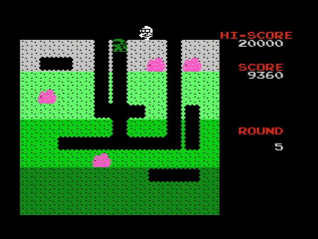
The NES has 2kiB of video RAM, one eighth of the MSX1. It also, though, has 256 bytes of OAM (object attribute memory in NES language, or sprite data to use more common terminology), and 32 bytes of palette RAM that aren’t included in that 2kiB. So, what does Dig Dug, released by the same company in the same time period, look like on the NES?
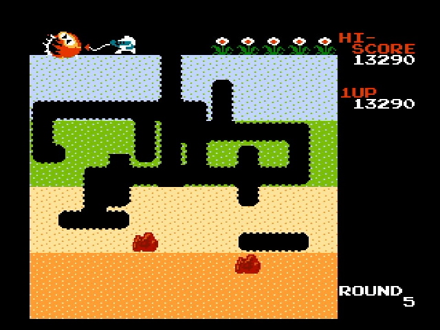
MSX fans are probably already writing in. After all, the NES has several big advantages over the MSX. In these screenshots alone, you have:
- Three-color sprites (vs. monochrome on the MSX1)
- Up to eight sprites per scanline (vs. 4 on the MSX1)
- Higher vertical resolution
- More colorful tilemap
However, all of these should actually be taking up more VRAM than the MSX, not less. Well, of course, what’s going on is well-known. The game Dig Dug uses CHR-ROM. A Dig Dug cartridge has an 8kiB ROM inside of it that’s hooked up directly to that video bus. So to say “the MSX1 has 16kiB of VRAM, the NES has <2kiB” is really not being a fair comparison. The MSX fans have a point.
But that has an important, key implication: to make CHR-ROM possible, the NES exposes the video bus over the cartridge slot. It looks like this: (Well, this is the Famicom)
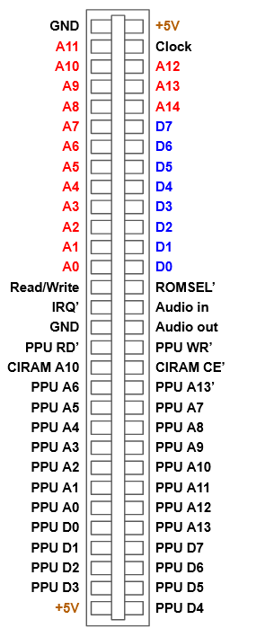
There’s a lot more signals to play with here than even the Master System. Most importantly, though, are those labeled PPU. They refer to the Picture Processing Unit, the NES’ graphics chip, and are hooked up directly to what on the MSX is an internal graphics bus. In fact, you can even put RAM on the board, and have the benefits of modifiable-on-the-fly VRAM. (And if you want, even bankswitch it) Unlike the Neo Geo, the NES was designed for this usecase, and the RAM can be modified in the same way as the VRAM that is built into the NES. (Which is used for tile maps and the like) This is typically called CHR-RAM.
Discrete logic
Let’s take a closer look at CNROM. This is just an example, and there are many mappers like it– what they have in common is that they’re built out of discrete logic, like Sega’s Dottori-kun arcade board, but usually they try not to use more than one or two chips. Here’s a closer look at Championship Bowling.
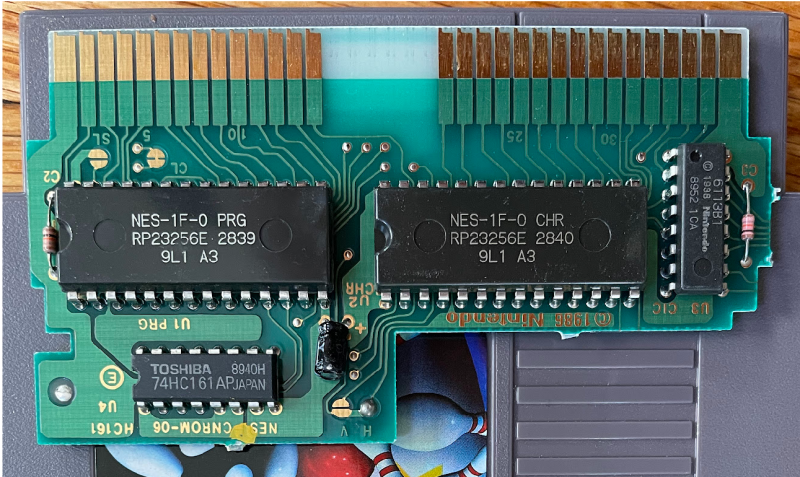
The two ROMs are the program and character ROM, and the small Nintendo-branded chip is the lockout chip. This board uses 32kiB of program ROM, so there’s nothing particularly interesting there. What’s interesting is the 74HC161. This is a standard chip; it’s a binary counter.
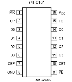
However, its clock input CP is not actually connected to anything, so the count will never increase. And so this is configured as a simple latch; a value stored on the D0, D1, D2, D3 pins will be output on the Q0, Q1, Q2, and Q3 pins. The benefit is that the value is “latched”; the Q pins can keep outputting the same value that’s set on the D side during a brief period the chip is enabled.
How are they written? It’s simply enabled whenever any of the ROM region is written to. This means no logic is needed to choose an address, and ROM isn’t usually written to in day-to-day coding, since it can’t store a value. The downside of this simple single-discrete-chip approach, however, is bus conflicts; they can be worked around, however.
This is called bankswitching: Two of these pins are attached to two address lines of the character ROM. So the NES still only sees 8kiB at any given time, but it can be divided into four”pages” that can be swapped out by the program. And unlike, say, a CD-ROM or a floppy disk, loading pages of data is essentially instant; it responds very fast.
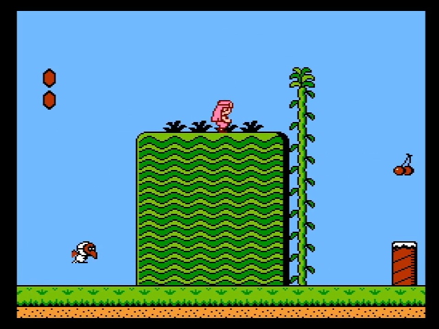
Fast enough, in fact, that games like Super Mario Bros. 2 (which is not CNROM, but just being used as an example because it’s widely recognizable, and was released on multiple mappers) can actually animate themselves just by switching out banks. This allows for things like the tufts of grass and the leaves on the climbing vines.
Compare to its Famicom Disk System counterpart, Yume Koujou: Doki Doki Panic, and you’ll find a much more stationary game. This is because the Disk System game uses VRAM (as do all disk system games), and doesn’t have time to copy that much data into RAM during the short vertical blanking interval. With bankswitching, it takes no time at all, and allows a lot of the world to move.
UNROM and Bankswitched PRG
Here’s Rush ‘n’ Attack, a game that uses the UNROM PCB. This game PCB uses 8kiB of CHR-RAM, but also has bankswitching for the program ROM. Bankswitching the program ROM can have some additional complexity, which is why this board is a bit more complicated.
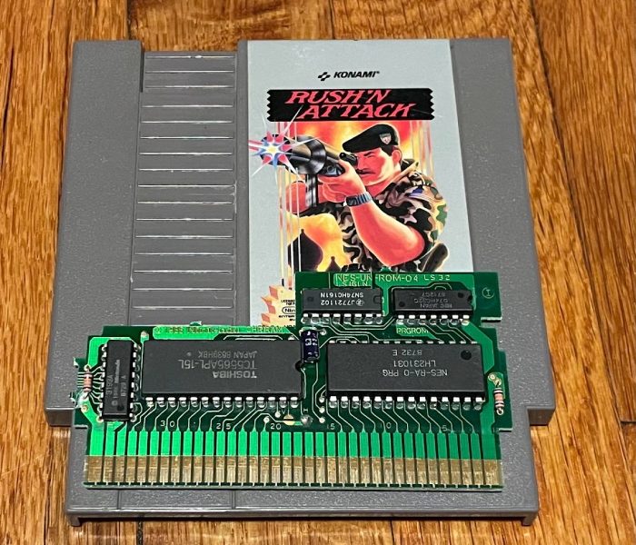
On the NES cartridge, typically there is a 32kiB window used for cartridge ROM. However, UNROM only has 16kiB of bankswitched ROM. The remaining 16kiB of the ROM are always available and in a known position between $C000-$FFFF. This is called a “fixed bank”. Why bother?
- Discrete logic (and many ASICs too) does not start up in a reliable state. Therefore, at bootup, which bank is selected is unpredictable. Since the NES always starts by looking at the reset vector at
$FFFC, having this part of ROM be fixed makes things more reliable. (For CHR, this isn’t as big of a deal, because the program can just make sure it sets the bank when it starts up) - Switching a page is instantaneous; this is nice for animations, but it also means that if you’re executing code from a bank that’s switched, you suddenly end up in the next bank. The processor doesn’t know about your bankswitching, though, and will just keep executing code from that same address in the new bank. If your bankswitching happens in a fixed portion, then you won’t have to worry about getting your code switched out from underneath you.
Discrete logic mappers continued to be used throughout the NES’ life due to their low cost and simple implementation. I don’t want to give the impression that they ceased to exist; in fact, most types of boards continued to coexist. New NROM games, without a mapper of any sort, came out as late as 1993, with Namco’s Ms. Pac-Man.
ASIC Mappers
Once we go beyond the simpler discrete logic-based circuitboards, we can start to look at some of the more elaborate possibilities that ASIC mappers open up. On the other hand, though, I don’t want to imply that discrete logic can’t be used to create elaborate circuits. And on the third hand coming out of my chest, there are a lot of different boards and different chips out there. So I’ve decided to limit the rest of this post into looking at the Nintendo MMC series, which among the ASIC-based mappers are definitely the most common.
ASIC just means “application-specific integrated circuit”; this is a common industry term referring to creating a dedicated chip rather than piecing it together out of general-purpose chips. Arguably even the NES’ PPU and CPU are ASICs.
The Nintendo MMC1
The Nintendo MMC1 began appearing in cartridges in the first half of 1987. Here it is on Culture Brain’s Hiryuu no Ken II; it’s an “SLROM” board, which means that in addition to an MMC1, it has both program ROM and character ROM, but no additional RAM. For variety’s sake, this is a Famicom game, and as a result, does not have a lockout chip– you might be forgiven for thinking it did, though, if you didn’t look closely at that small Nintendo IC. But it has too many pins for that.
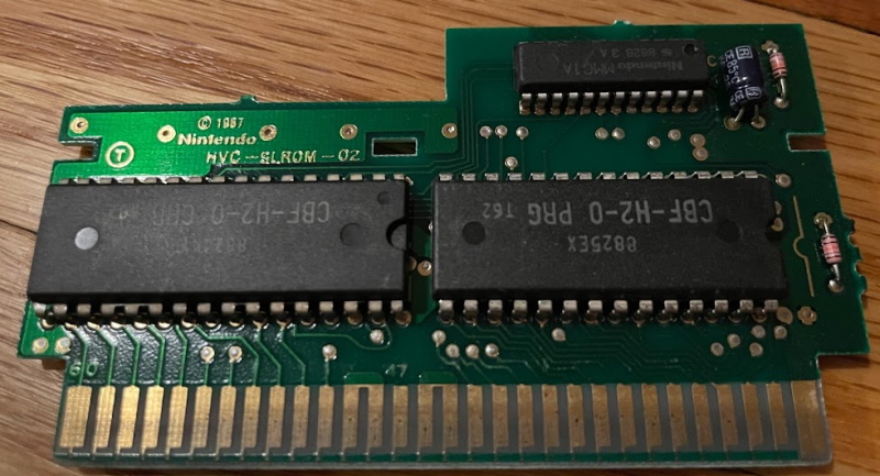
The Nintendo MMC1 is a small chip which controls a lot of lines. It seems that in order to reduce the number of required pins, it’s actually communicated with in a serial fashion through a shift register, one bit at a time. Later MMC chips would “bite the bullet” and use larger packages instead, though it’s worth noting that any NES programmer should be used to dealing with shift registers; that’s how controllers are read.
In terms of capabilities, it’s primarily about bank-switching, as well as the capability of manipulating the other control lines. For example, the VRAM of the NES is so small, that it can only scroll smoothly horizontally or vertically, but not both. (This is called “nametable mirroring”, and uses the CIRAM pins.) On mapper-less or simpler cartridges, this was set in hardware; for example, since Aspect Star “N” only has vertical scrolling, it uses horizontal mirroring. You can see a solder blob on the upper left of the RetroStage PCB I used.
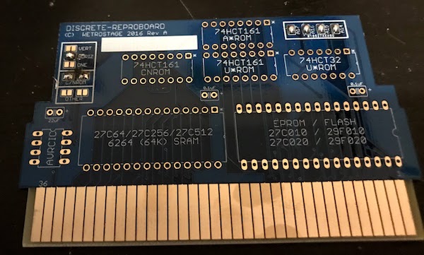
The MMC1 through its control circuit can not only control multiple switchable program and character ROM banks, it can change the mirroring on the fly. This allows for games like Kid Icarus (the first MMC1 game) and Metroid, where hallways can go vertically or horizontally, but never both.
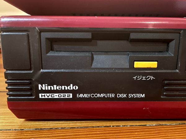
One thing I’m not sure about is if MMC1 was particularly designed for Famicom Disk System ports. The Famicom Disk System also allowed games to switch their mirroring on the fly, and this was necessary for gameplay. But it also had other functions the MMC1 did not duplicate, like timers and its extra sound channels. (While that last one wasn’t an option in North America or Europe, it could’ve been done for Japan)
There was another Disk System feature that MMC1 brought to the cartridge system. Look at this cartridge circuit board (Ultima: Exodus, which was not a Disk System port, but it’s the same one used by The Legend of Zelda, which was) and see if you can figure it out.
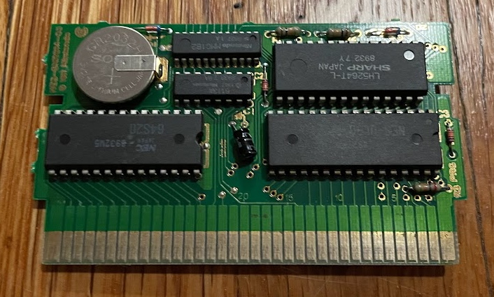
That’s right: saved games, in this case courtesy of battery-backed SRAM rather than a floppy disk. As far as I know there’s no reason technically that earlier games with on-cartridge SRAM couldn’t have saved it with a battery, but it was the MMC1 games that actually brought out that capability. One exception is the mapperless Family BASIC, released only in Japan, and had the option of using a standard AA cell battery to save its RAM.
By your powers combined
One use of MMC1 you might not expect is in one of the most common NES games of all time, Super Mario Bros./Duck Hunt/World Class Track Meet, which was sold alongside the “Power Set”, which included the NES console, a Zapper light gun, and the Power Pad peripheral. The three-game multicart includes games for both of these accessories; and of course, the must-have Super Mario Bros..
All of these games were released separately without mappers at all, except for World Class Track Meet, which used the simple discrete-logic CNROM, much like Championship Bowling.
| Mapper | Mirroring | PRG ROM | CHR ROM | |
|---|---|---|---|---|
| Super Mario Bros | NROM | V | 32 kiB | 8 kiB |
| Duck Hunt | NROM | V | 16 kiB | 8 kiB |
| World Class Track Meet | CNROM | H | 32 kiB | 32 kiB |
| Total | MMC1 | Switchable | 128kiB | 64kiB |
MMC1 offers the ability to do the proper bankswitching to include the more complex CNROM game World Class Track Meet; the previous Super Mario Bros./Duck Hunt multi-cart used a simpler discrete logic board.
You might notice that the board offers way too much ROM space. In the CHR-ROM, many of these pages are empty, but one of them contains what appears to be the background graphics of Super Mario Bros. 2 for the Famicom Disk System. TCRF has some codes to let you use them in Super Mario Bros., but of course that does result in some glitches.
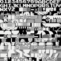
I’m not sure why this is there; perhaps they were considering an MMC1 conversion of Super Mario Bros. 2’s Japanese version at some time, but it’s worth noting that these tiles are after the tiles of the select screen, while all playable games are before. Could Super Mario Bros./Duck Hunt/World Class Track Meet have had a fourth game? I guess we’ll never be sure. Super Mario Bros 2 would’ve required additional work to port above and beyond the existing games, being designed to load data from disk as well as using the FDS’ timer, but given that other disk system game ports used MMC1 it seems possible, and the timer could be worked around.
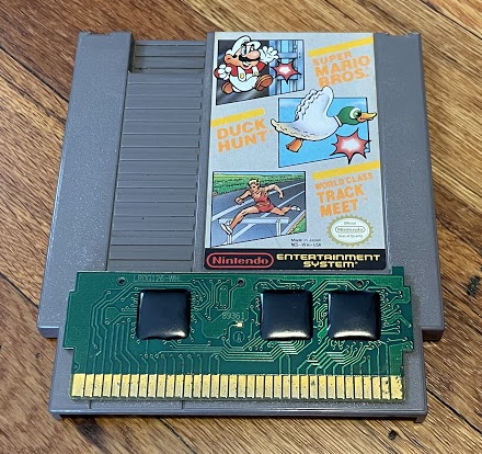
One other thing of interest about this game is that because it was produced in such high quantities, it uses “chip-on-board” or “epoxy blob” technology. Thankfully, use of this technology is fairly rare among Nintendo-manufactured boards of this period, only being seen in the very most popular or most manufactured boards. You do see it on some non-Nintendo manufactured Famicom games, though.
Nintendo MMC2
MMC1 was used in a lot of games. 390, if the NESdev wiki is to be trusted. So what about MMC2? It’s used in a whopping… one. But hey, if you’re going to be used in one game, at least be used in a good one.
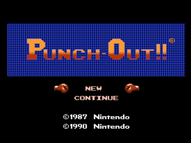
Punch-Out!!, or Mike Tyson’s Punch-Out!! if you were early to the party, is an NES boxing title that has the good timing to come out at a high point of interest in the sport, and also the luck of being a good game. Well, that part might not be luck.
If you haven’t played it, it’s a behind-the-shoulder boxing game where you control the underdog fighter Little Mac as he rises up the ranks and defeats a series of colorful and cartoonish boxers, ending up with Mike Tyson himself Mr. Dream who isn’t Mike Tyson at all what are you talking about. I’m not very good at it, though, so expect to see the first fight.
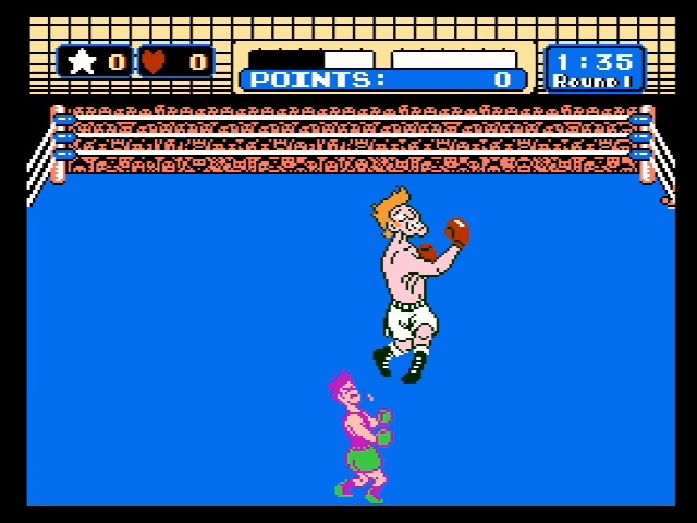
The MMC2 can bankswitch both program ROM and character ROM, with two switchable banks for background and sprites. The program ROM is a bit interesting, with the 32kiB window divided into a 24kiB fixed block and only 8kiB that can be banked. But the most interesting thing about MMC2 is its character ROM handling.
So when we talked about bankswitching CHR-ROM, it’s important to note that at any given time, the PPU can only “see” 8kiB of ROM. MMC1 and the discrete logic boards we’ve looked at have the bankswitching controlled by the CPU. This is fine if you’re changing banks for the whole screen at a time, like Super Mario Bros. 2, but what if you want to change banks mid-screen? You’d have to carefully time your code; none of the mappers we’ve seen so far have provided timers of any sort to help with that, either.
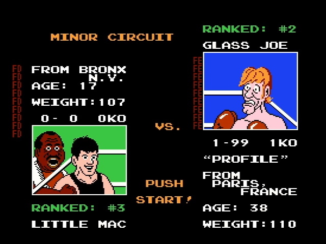
On Nintendo MMC2, however, the developer sets two banks at once for each of its CHR banks using the CPU as usual. Then, two special tiles, $FD and $FE, allow rapid switching between them– this is because the MMC2 has access to the CHR bus mentioned before. The CPU doesn’t have to be involved at the moment of bankswitching; the presence of the tile tells the mapper all it needs to know. Let’s see how this looks in practice.
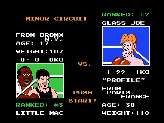
On this screen, Little Mac and Glass Joe compare stats. The interesting thing is that Joe and Mac are in different banks, while the text shares a bank with Mac. You can drive this home by looking at the screen in a nametable viewer in an emulator like FCEUX.
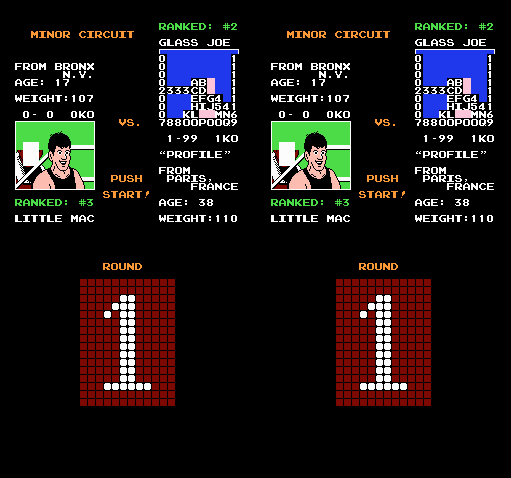
MMC2, however, allows bankswitching within a line with ease. Let’s use a hacked ROM to make FD and FE visible. (Note that in some cases the palette made my edited tiles not appear, so I have manipulated this screenshot to make it more clear)
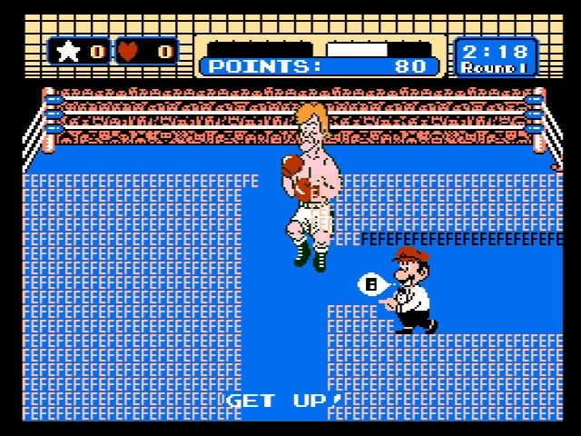
One other place it’s used is for the “GET UP!” message when Little Mac is knocked out and Mario starts the count. (This screenshot is not manipulated, beyond the hacked ROM)
This fully PPU-controlled bankswitching feature doesn’t actually get used too much, which may be why MMC2 was never picked up again for later titles. Still, it definitely had its use for this game, and with the sales success of Punch-Out!!, that may have been enough to justify its existence.
Ooops a digression: the Namco 109
It’s commonly believed that while in Japan, Famicom publishers could do whatever they wanted and use whatever chips they wished, in America and Europe, Nintendo strictly limited them to using their in-house mappers. And it’s true that Nintendo did require that all licensees have their games manufactured in-house. But if that mapper requirement was true, how do you explain this?
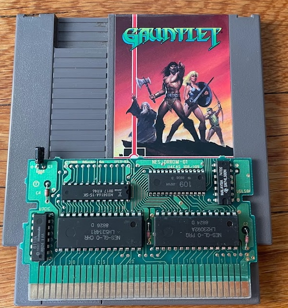
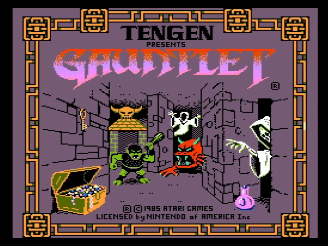
This is the NES-DRROM, manufactured by Nintendo for the Tengen game Gauntlet. While Tengen would go on to make their own boards in violation of Nintendo’s licensing, this game is from the brief era in which they were Nintendo licensees, and the two chips on it are rather interesting.
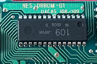
First, the Namco 109. (Sometimes called the Namcot 109) This is part of a seemingly-identical series of Namco mappers, the 108, 109, 118 or 119. What they have in common is sophisticated PRG and CHR banking, with four switchable PRG banks, and a whopping 6 simultaneous switchable CHR banks: 2 in the $0xxx region used typically by backgrounds, and 4 in the $1xxx region of CHR-ROM typically used by sprites.
If you’re only familiar with the NES, you might be surprised to see a Namco chip; something this specific is unlikely to be useful for systems that aren’t the Famicom as far as I know. While licensing prevented Namco from publishing NES games under their own label until very late in the console’s life, it was one of the largest and most prolific Famicom developers, where the licensing was much looser and Namco could manufacture their own boards and chips in-house. They also sold their chips to other developers, and this one in particular seems to have been used quite a lot, especially in Japan.
What about the other chip?
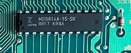
NESCardDB reports this as a 2kiB SRAM. There’s no battery for power, and this is actually attached to the CHR bus– but there’s also a CHR-ROM. In this case, the RAM is actually being used to provide additional nametables. While the NES has the capability for four screens’ worth of nametables, it only has enough RAM for two; this is the reason for the mirroring mentioned above. But by adding this extra RAM, any need for mirroring at all is eliminated. (The Namcot 109 doesn’t actually allow you to control mirroring, but this would be unnecessary here anyway)
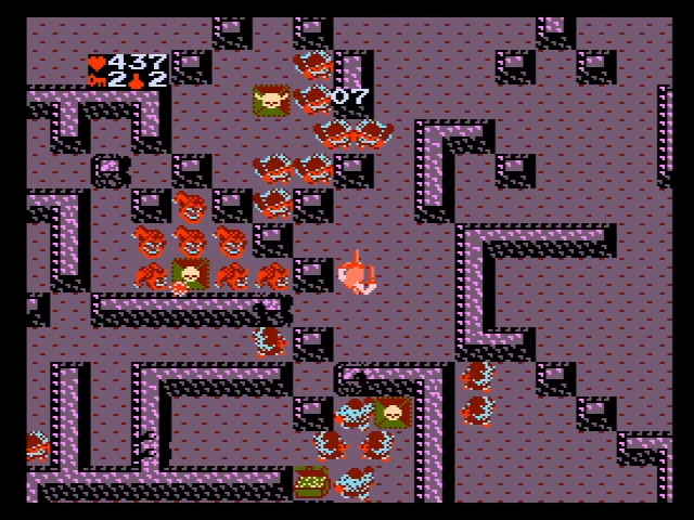
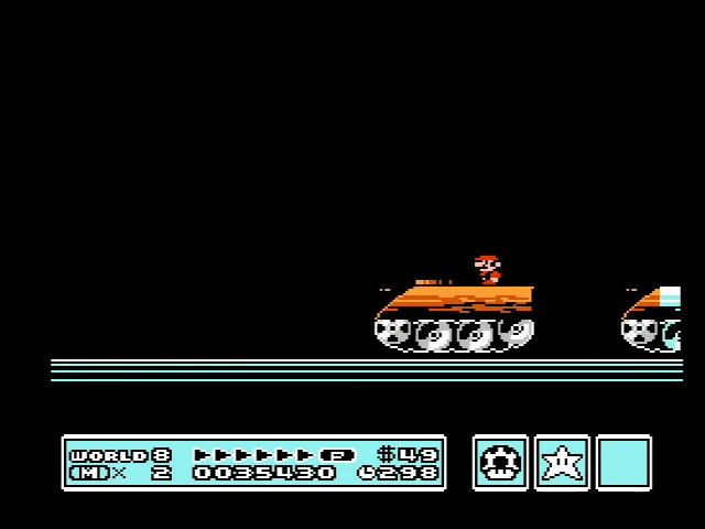
This extra RAM makes Gauntlet, a port of the arcade classic, possible. The game has scrolling in two-directions. With four nametables instead of two, Gauntlet avoids the attribute glitches on the right side of the screen in Super Mario Bros. 3 (below); and indeed, since the game’s levels are the same size as the nametables: it doesn’t need to do any fancy code to load new parts of the level, and it can load it all at once.
Let’s take a look at those nametables.
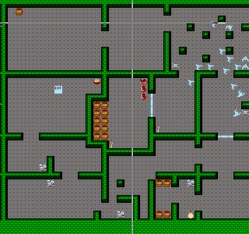
Notice that the enemies show up here. Gauntlet is willing to go to such lengths to avoid scrolling; it actually uses software sprites to avoid flicker. And this explains why it goes to such lengths to avoid scrolling: unlike sprites, the tilemap on the NES can only be changed using the slower CHR-RAM process mentioned above, so freeing up vblank time from scrolling gives the game more time to move enemies. And it still does have slowdown despite this.
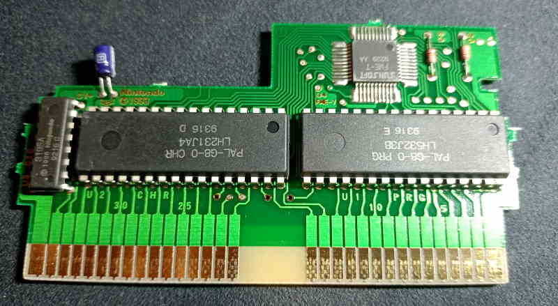
Tengen wasn’t the only one to use a Namco 109 chip in a US release; the first seems to be Data East’s Ring King in 1987, a port of Namco’s Family Boxing. (This version did not have the extra nametable RAM, so didn’t have the four-screen mirroring, but since it’s a boxing game, it didn’t need it) Sunsoft would also bring their own mappers to Nintendo-manufacturered boards for Batman: Return of the Joker and the (in)famous Scandinavian exclusive Mr. Gimmick, pictured below. (Special thanks to Retro Gamer Paradise for the PCB photo!)
So why did some companies, like Konami, prefer to switch to Nintendo-made mappers for the US releases of games? Well, I don’t have access to the licensing agreements Nintendo had their partners sign, but my guess is that it just came down to money. Tengen would switch to manufacturing their own games outside of Nintendo’s licensing system at the end of 1988, so perhaps the situation that produced Gauntlet wasn’t stable. (And that’s a fascinating story of its own)
Nintendo MMC3
Another thing came along in the end of 1988: the MMC3 enhancement chip. This chip powered a lot of the console’s mega-hits, including Super Mario Bros. 3, the American Super Mario Bros. 2, Adventure Island IV, Shadowgate, Kirby’s Adventure, and the last licensed NES game in North America, Wario’s Woods. NESdev claims a list of 300 titles. Not as many as MMC1, but not too shabby.
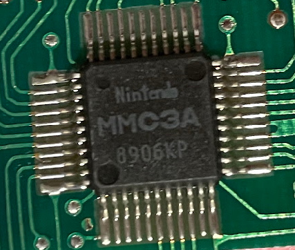
The MMC3 pictured above comes from the game Legacy of the Wizard, whose Japanese version, Dragon Slayer 4: Drasle Family used a Namco 109 chip just like Gauntlet, though it didn’t have the additional nametable RAM. As it turns out, the MMC3’s PRG and CHR banking match the Namco 108 family. From its release in the fourth quarter of 1988, MMC3 began to be used for games ported from the Namco 108 chips.
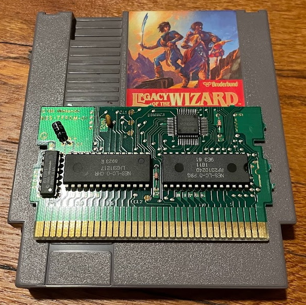
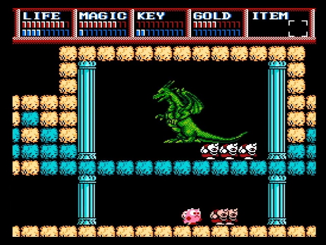
Legacy of the Wizard is a really fun game, but it doesn’t use many of the more advanced features of the MMC3. The Namcot 108 series only features bankswitching; it can’t even control nametable mirroring like the MMC1 did. The MMC3 can control mirroring and many other features; but since Legacy of the Wizard stays quite close to its Japanese original, we’ll need to look for a different game to show them off.
Rare’s High Speed
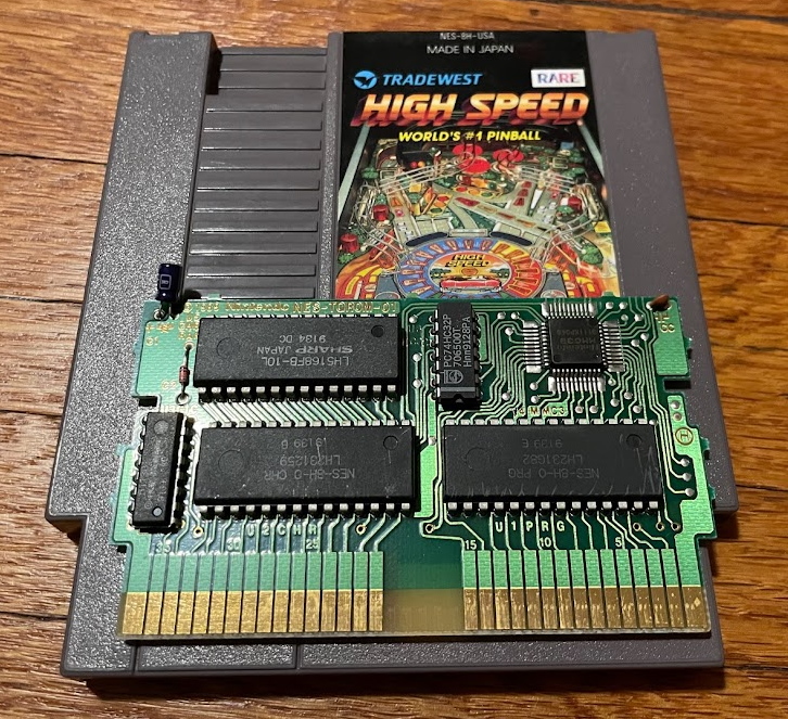
Here’s Rare’s High Speed. It’s a pinball video game, and we all know how I like pinball. But you might also notice the circuitboard is a bit more complex than the Legacy of the Wizard board. This circuitboard, NES-TQROM, was only used by two games, both pinball conversions by Rare, and has the very interesting feature of the Sharp RAM chip.
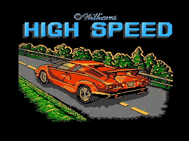
While the MMC3 could support additional program RAM, used in games like Super Mario Bros. 3 or with battery backup in games like Kirby’s Adventure, or four nametables, like in Rad Racer II, this game uses the additional RAM to have simultaneously both CHR-RAM and CHR-ROM. Both can be banked simultaneously alongside each other; much of the game uses CHR-RAM for sprites like the ball, while also using ROM elsewhere, especially for the background. This feature did require an additional 74HC32 discrete logic OR chip to provide a chip select signal, so it goes beyond the stock MMC3 by one logic gate.
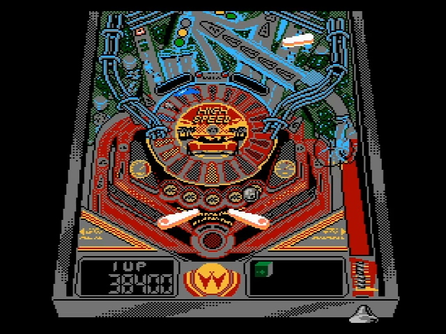
So first impressions off the bat are that High Speed looks great on NES, if perhaps a little busy. But there is an immortal problem of bringing pinball to game consoles. Pinball machines are pretty much always vertically oriented; this is due to gravity. Home televisions are oriented horizontally, and people rarely are willing to use tate mode. The 1978 Sears Pinball Breakaway solved this by changing the proportions. But this game needs to stick to the proportions of the real machine it’s based off of.
How does it solve the verticality problem?
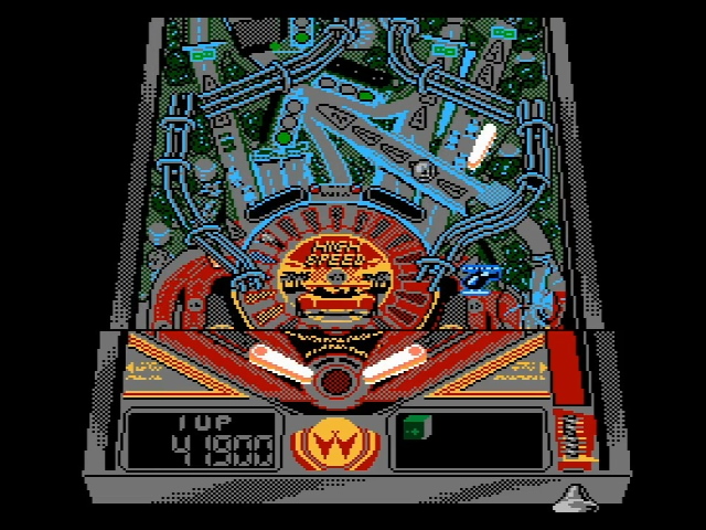
Scrolling, of course! Well, I say, “of course”, but there are actually plenty of quite good flip-screen pinball games. The problem of scrolling pinball, you see, is that it results in the flippers moving on the screen; the player really wants to be focused on the flippers, so it helps if they’re in the same place. High Speed splits the difference by focusing you on the bottom of the screen where the main flippers are, but the secondary flipper does move.
But you might be thinking. “Hey Nicole! That’s a lot of tiles on screen. And those are pretty detailed, so it’s not like clever reuse can get you that far” And you’d be right! Let’s take a look at the nametables. These were, as usual, taken using the FCEUX emulator; the white bar represents where the scanline on the screen is. Basically you can think of this as a picture of what the nametables look like to the PPU when it’s drawing at the white bar.
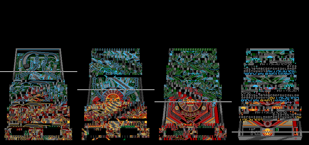
The game is rapidly switching out the nametable four times per screen. Unlike the MMC2, on the MMC3 the CPU still has to handle all the bankswitching itself, but it has another trick up its sleeve: the IRQ. The 6502 has no multithreading or multicore capability, but has interrupt capability: a pin on the CPU that can receive a signal that will force it to drop what it’s doing and run a separate process, called an interrupt handler. The 6502 has two interrupts on board.
On the NES, one of the two interrupts, the NMI (non-maskable interrupt, but the non-maskableness of it isn’t very important today), is hooked up to the PPU, and can be used to let the CPU know when the PPU is in vblank. This is generally very important for reasons discussed above. The IRQ, however, is available on the cartridge slot. This is another “secret power” of the Famicom design, allowing the cartridge to keep track of things the processor can’t.
Have you seen Ben Eater’s YouTube video on creating a video card? The Nintendo PPU is quite a bit more complex, but both that and Ben’s homebrew card have something in common: they are built around a series of timers. A television signal must produce certain pulses at certain times, and the data for certain lines at certain times.
The key thing about this is that it means that it’s very reliable on when it does certain things. For example, let’s take a simple screen from Aspect Star “N”. This screen is showing a glitch, but it doesn’t matter.
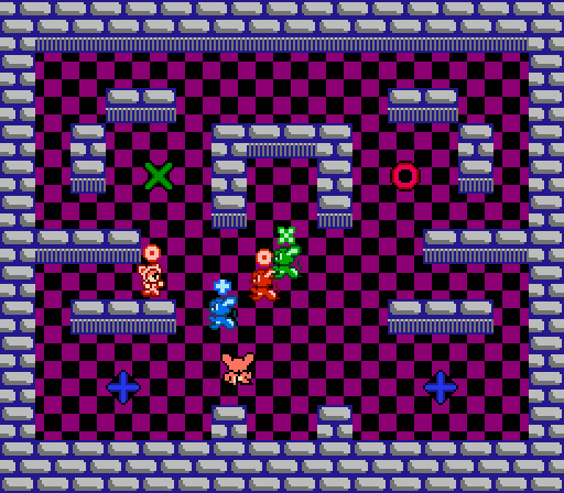
All of the tiles forming the level are the tilemap, and are made out of tiles in the block $0000-$0FFF. So the PPU must access those tiles when drawing the screen. Nicole, the aspect markers, and the four enemies are all drawn using sprites, and the sprites in this game are stored in the area $1000-$1FFF. The PPU fetches the sprites for each line separately from the tile, and most crucially, always fetches something, even when there are no sprites on that line. Because it’s just a series of timers and counters.
The MMC3 uses this knowledge to provide a scanline counter. If a game uses backgrounds in the first half of the 8kiB CHR zone, and sprites from the second half– as most games do, and as the MMC3 CHR layout encourages– then you can detect when it goes from fetching tiles, to when it fetches sprites, just by seeing when fetches go above $1000. This means looking at the PPU address line A12, which is right there on the cartridge edge.
Now of course, this is a bit of a delicate dance, and it can be broken. But if care is used, a scanline counter can be set, that is decremented each time that A12 line change occurs (with some in-chip filtering to eliminate false positives). When the counter reaches zero, it will fire an IRQ, and if the dance succeeded, that will have been the number of lines you set in the counter. You can see how this allows High Speed to use far more tiles for its tilemap than should be possible; it’s also used for the status bar in Super Mario Bros. 3. (Where there are some minor glitches often visible at the seam, like above the text “World 8” here)
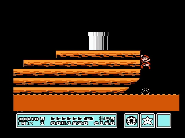
The MMC3 appeared at the end of 1988. This is a time when Nintendo started to see increasing competition from the Sega Master System; the Sega Master System also has a scanline counter and interrupt. You can’t really say that Nintendo “stole” the idea (similar timing concepts definitely predate Sega’s console; including on the Famicom Disk System, though that wasn’t tied to scanlines), but it’s possible that they were implemented only now because competition were heating up on the market.
MMC4
The MMC3 did not have the MMC2’s “change CHR banks using a magic tile” trick. However, Nintendo brought that back with the MMC4. In fact, the MMC4 is pretty much identical in capabilities to the MMC2, except the program ROM banking is structured differently, and there are some minor technical implementation differences.
But you won’t see any MMC4 games in the west. As far as I know, just three titles used it:
- Famicom Wars
- Fire Emblem
- Fire Emblem Gaiden
What do all of these games have in common? Despite their modern successors having huge western fanbases, during the NES era they never left Japan. Another thing all these games have in common is the heavy use of Japanese-language text.
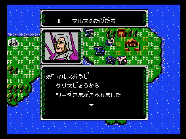
Unlike Punch-Out!!, the FD and FE tiles aren’t always blank. In this game, Fire Emblem, they form the borders of textboxes; this makes perfect sense, allowing the game to switch in a different bank for text and character portraits. The game has both hiragana and katakana, which use a lot of the CHR space.
MMC4 does not have the scanline IRQ feature that MMC3 had, though, which may explain why it wasn’t used as often by developers. Or perhaps it just was exclusive for Intelligent Systems, and they didn’t want to share.
Nintendo MMC5
We already saw one MMC5 game mentioned; the beefy Metal Slader Glory. MMC5 is definitely the most advanced Nintendo mapper, and possibly is the most advanced mapper to be used by anyone on the NES. For example, it doesn’t have a single bankswitching layout. It has multiple, which can be selected and even switched on the fly. It uses a deep knowledge of the internal state of the NES to allow for graphics tricks that were unthinkable at the system’s release. It even has expansion audio, though since this board (Laser Invasion by Konami) is a North American release, it won’t be hooked up.
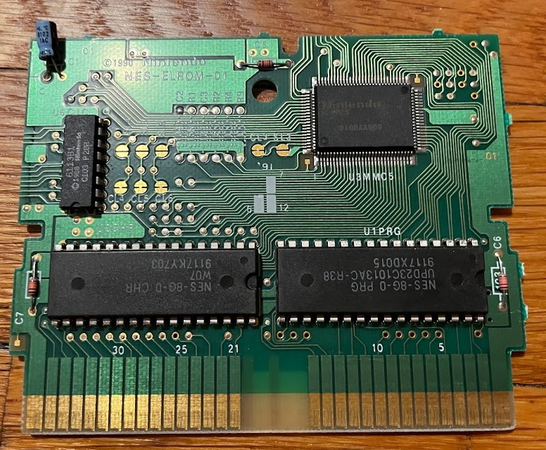
The MMC5 is the only Nintendo MMC chip that doesn’t just augment the capabilities of the PPU, it augments the CPU beyond just bankswitching. It features a built in 8-bit multiplier (16-bit output); the 6502 can’t do multiplication natively, so there are definitely cases where this will speed things up. This sort of CPU assistance would become a lot more popular on the Super Nintendo.
The first MMC5 game seems to have been Nobunaga’s Ambition II, released in Japan in February of 1990. The SNES came out in Japan at the end of that year, so there was only a limited window in which the MMC5 was the best home hardware Nintendo had.
Expanded attributes
So what kind of tricks were up the MMC5’s sleeve? Well, let’s take a look at a tactical battle in Nobunaga’s Ambition II to start.
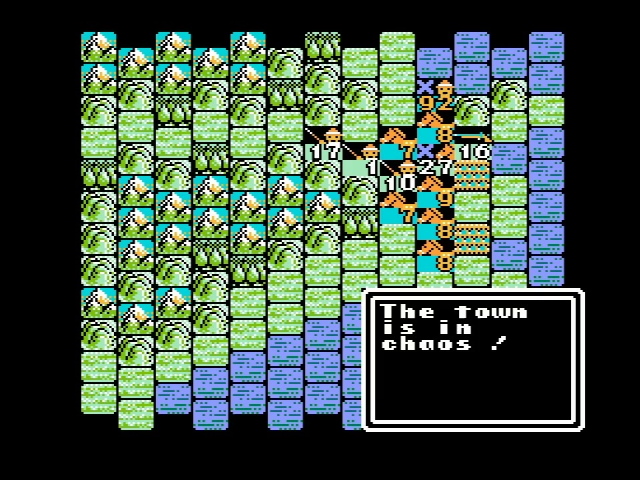
Now, if you’re familiar with the NES hardware, you might already see what’s impressive. But if you’re not, let’s go into a bit of detail about attribute tables. See, the NES tilemap is made out of 8x8 tiles, each of which can have four colors from a set of four palettes. Let’s take a look at Aspect Star “N”. I’ve died, which will limit the number of sprites on screen. The main thing to look at is the tilemap under the 16x16 grid.
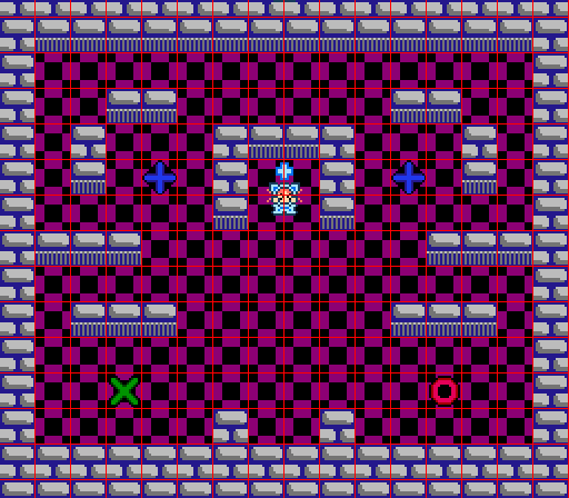
Notice that things like the Aspect tiles have their own palette, but are limited to their own 16x16 region. The only thing that crosses these barriers are the sprites that Nicole is made out of. This is called the “attribute table” on the NES; you can only change the colors of the tilemap within a 16x16 block. This is a major reason so many things on NES games are 16x16 tiles in size. Whereas in Nobunaga’s Ambition II, things are different.
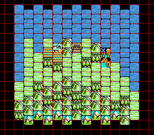
Notice that there’s no way to arrange the 16x16 grid so that it lines up with the tilemap palettes. The attributes are no longer 16x16, but are now 8x8, the same size as the tiles. How did they manage this?
The PPU attribute tables are just a part of the nametables; they’re at the end, but they’re at known spots in RAM. That RAM is, of course, accessed over the PPU bus. It turns out that the PPU fetches a palette for each 8x8 tile. The MMC5 keeps very close track of the PPU timing, so it knows when to swap out for the palette it wants; it can even change the CHR bank on the fly for each tile as well. This allows for a huge number of tiles on screen, and for more advanced color patterns. (A downside, though, is that the same expansion table is used for every nametable)
Vertical split mode and scanline timing
Another fun party trick the MMC5 can play with its expansion RAM is the use of a vertically split mode, by keeping track of each scanline, and swapping out which nametable to read from when a certain horizontal point is reached. A downside here is that it doesn’t interact particularly well with horizontal scrolling, but it’s still good enough to put a cool effect at the beginning of HAL Laboratory’s Uchuu Keibitai SDF.
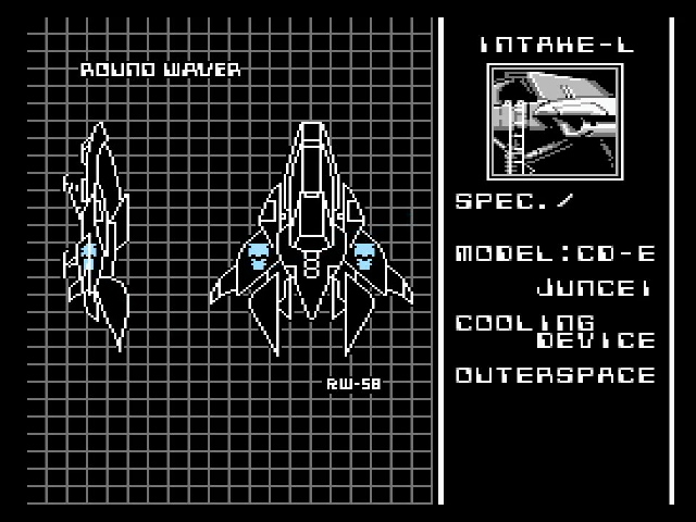
The scanline detection of the MMC5 is much more accurate than the MMC3, since instead of relying on the PPU switching from nametables to sprites and looking at just one address line, it relies on close examination of nametable fetches. This requires more logic and a more complex circuit, but it allows for a much more accurate timer.
As a result, MMC5 doesn’t technically have a scanline counter. It actually has a direct scanline IRQ. Instead of counting down from a particular point, you just tell MMC5 which scanline you want an interrupt on. Notice that the Super Mario Bros. 3 screenshot above had some glitchiness at the seam, which Rare was able to avoid through careful timing. Meanwhile, look at this neat takeoff sequence from Laser Invasion.
Those are some very impressive visuals for the humble NES, and they’re made possible by the highly accurate scanline timing of MMC5.
The MMC5 has a number of other features as well, including timers added in the MMC5A variant. This is just a taste; unfortunately, due to its expense and late release, MMC5 was not nearly as widely used as MMC1 or MMC3; NESdev claims only 15 games.
Nintendo MMC6
The MMC line ends on kind of an uninteresting note. The MMC6 is just a variant of the MMC3, used in StarTropics and StarTropics II. It supports less save RAM; only 1kiB vs. 8kiB. That’s about it.
Oh, and one other thing. Ever seen this label on an NES cart?
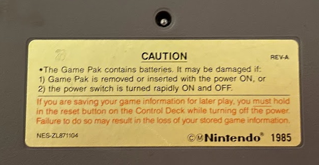
Why did you need to hold RESET while turning off the power? Well, the power switch on the NES just cuts off the power supply. As the 6502 loses power, it will continue to try to run its program, and can for a brief period run in an unpredictable mode where it could write to the wrong address or do other unpredictable things. This isn’t a big deal; unless it happens to write to those magic addresses that are battery-backed. Then it could corrupt your saved games. Holding RESET basically puts the processor in a stasis where it won’t do anything unpredictable.
The MMC6, on the other hand, has a special address which allows it to protect the memory. At this point to corrupt the memory the NES would have to first hit the protect address by chance, and then hit the memory; this is much more unlikely, and the StarTropics manual removes the ubiquitous warning about holding in the RESET button.
MMC6 and MMC3 are so similar that the ubiquitous INES standard for ROM headers doesn’t actually distinguish the two. However, this can cause issues with the sound driver in the game Low G Man; the issue was obscure enough that it was missed during the standard’s creation.
And that’s the last MMC chip!
A quick digression on the Super Nintendo
The Super Nintendo does not expose the S-PPU over the cartridge slot like the NES did. Instead, it has 64kiB of VRAM, which is definitely nothing to sneeze at. The S-PPU is arguably one of the most powerful graphics chips of the 16-bit console generation, with its Mode 7 even surpassing the mighty Neo Geo in some ways by having scaling and enlarging of a single tilemap. So instead, SNES expansion chips tended to augment the CPU, using things like digital signal processor chips to perform calculations faster than the sluggish 3.5MHz 65C816 could.
Still, over time even the S-PPU stuttered with the demands of 3D graphics. Star Fox famously introduced the SuperFX chip (codenamed “Mario”) to deal with this and provide some impressive polygonal graphics at a less impressive frame rate.
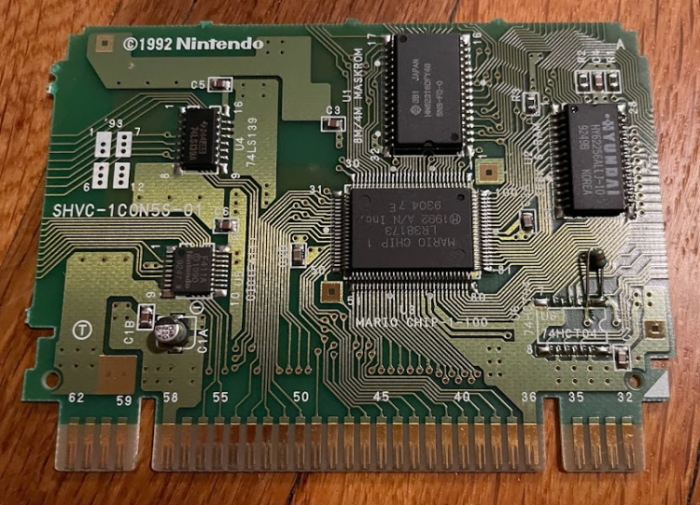
Without access to the PPU bus, how does the SuperFX work? It renders to a block of RAM, and then the CPU’s job is to copy that block into the VRAM. An NES game that used a similar technique of offloading its rendering could in theory provide faster results by using the PPU bus; one example I know of that goes further than MMC5 is YouTube user TheRasteri’s homebrew port of Doom using a Raspberry Pi. After looking into what expansion chips on the NES did during the system’s life, I can’t really say it’s cheating here. Nintendo would’ve done the same thing if they had the opportunity.
